Civil Rights
Movements, leaders, victories and the continuing fight for equality.

Explore the people, places, events, achievements, struggles and stories that shaped our journey.
Movements, leaders, victories and the continuing fight for equality.
Innovation, patents, science, technology and world-changing contributions.
Pioneers, champions, Negro Leagues, records, activism and excellence.
Meet the people whose lives, choices and achievements shaped the journey.
Black towns, communities, institutions and places where history happened.
Moments that changed communities, movements, institutions and the nation.
In August 1908, a white mob attacked Springfield, Illinois’s Black community, destroying homes and businesses and lynching two Black men. National outrage over the violence helped spur the movement that created the NAACP the following year.
MORE →Reflects the personal views, recollections, and perspective of the author, Mike Davis.
This is a personal recollection on the Move fire on May 13, 1985
| General information | |
|---|---|
| Launched | October 12, 2011 |
| Common manufacturer | |
| Physical specifications | |
| Socket | |
| Architecture and classification | |
| Technology node | 32 nm |
| Instruction set | x86-64-v2 |
| Products, models, variants | |
| Core names | |
| History | |
| Predecessor | Family 10h (K10) |
| Successor | Piledriver - Family 15h (2nd-gen) |
The AMD Bulldozer Family 15h is a microprocessor microarchitecture for the FX and Opteron line of processors, developed by AMD for the desktop and server markets.[1][2] Bulldozer is the codename for this family of microarchitectures. It was released on October 12, 2011, as the successor to the K10 microarchitecture.
Bulldozer is designed from scratch, not a development of earlier processors.[3] The core is specifically aimed at computing products with TDPs of 10 to 125 watts. AMD claims dramatic performance-per-watt efficiency improvements in high-performance computing (HPC) applications with Bulldozer cores.
The Bulldozer cores support most of the instruction sets implemented by Intel processors (Sandy Bridge) available at its introduction (including SSSE3, SSE4.1, SSE4.2, AES, CLMUL, and AVX) as well as new instruction sets proposed by AMD; ABM, XOP, FMA4 and F16C.[4][5] Only Bulldozer GEN4 (Excavator) supports AVX2 instruction sets.
According to AMD, Bulldozer-based CPUs are based on GlobalFoundries' 32 nm Silicon on insulator (SOI) process technology and reuses the approach of DEC for multitasking computer performance with the arguments that it, according to press notes, "balances dedicated and shared computer resources to provide a highly compact, high units count design that is easily replicated on a chip for performance scaling."[6] In other words, by eliminating some of the "redundant" elements that naturally creep into multicore designs, AMD has hoped to take better advantage of its hardware capabilities, while using less power.
Bulldozer-based implementations built on 32nm SOI with HKMG arrived in October 2011 for both servers and desktops. The server segment included the dual chip (16-core) Opteron processor codenamed Interlagos (for Socket G34) and single chip (4, 6 or 8 cores) Valencia (for Socket C32), while the Zambezi (4, 6 and 8 cores) targeted desktops on Socket AM3+.[7][8]
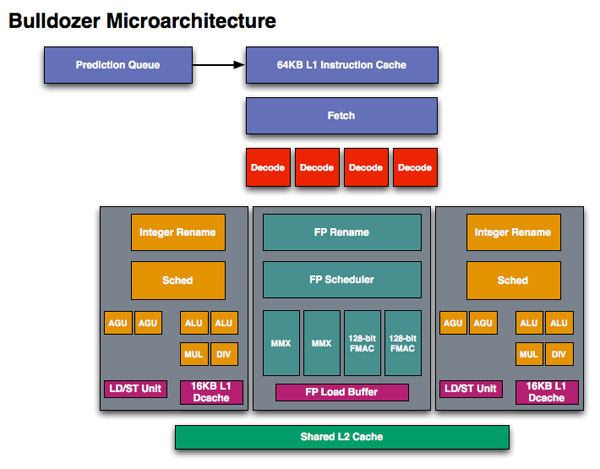
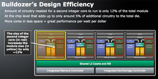
Bulldozer is the first major redesign of AMD’s processor architecture since 2003, when the firm launched its K8 processors, and also features two 128-bit FMA-capable FPUs which can be combined into one 256-bit FPU. This design is accompanied by two integer clusters, each with 4 pipelines (the fetch/decode stage is shared). Bulldozer also introduced shared L2 cache in the new architecture. AMD calls this design a "Module". A 16-core processor design would feature eight of these "modules",[9] but the operating system will recognize each "module" as two logical cores.
The modular architecture consists of multithreaded shared L2 cache and FlexFPU, which uses simultaneous multithreading. Each physical integer core, two per module, is single threaded, in contrast with Intel's Hyperthreading, where two virtual simultaneous threads share the resources of a single physical core.[10][11]
In a retrospective review, Jeremy Laird of APC magazine commented on Bulldozer issues, noted that it was slower than the outgoing Phenom II K10 design, and that the PC software ecosystem had not yet "embraced" the multi-threaded model. By his observation, these issues caused a substantial loss for AMD, and the company lost over 1 billion USD in 2012. Some industry observers were predicting the bankruptcy of AMD by mid-2015. The company later managed to return to profitability. Mentioned reasons for regaining profitability were the earlier divesting of in-house manufacturing into GlobalFoundries, the outsourcing of manufacturing to TSMC and the creation of a new Ryzen CPU design.[12]


Bulldozer made use of "Clustered Multithreading" (CMT), a technique where some parts of the processor are shared between two threads and some parts are unique for each thread. Prior examples of such an approach to unconventional multithreading can be traced way back to the 2005 Sun Microsystems' UltraSPARC T1 CPU. In terms of hardware complexity and functionality, a Bulldozer CMT module is equal to a dual-core processor in its integer calculation capabilities, and to either a single-core processor or a handicapped dual-core in terms of floating-point computational power, depending on whether the code is saturated in floating point instructions in both threads running on the same CMT module, and whether the FPU is performing 128-bit or 256-bit floating point operations. The reason for this is that for each two integer cores, that is, within the same module, there is a single floating-point unit consisting of a pair of 128-bit FMAC execution units.
CMT is in some way a simpler but similar design philosophy to SMT; both designs try to utilize execution units efficiently; in either method, when two threads compete for some execution pipelines, there is a loss in performance in one or more of the threads. Due to dedicated integer cores, the Bulldozer family modules performed roughly like a dual-core, dual-threaded processor during sections of code that were either wholly integer or a mix of integer and floating-point calculations; yet, due to the SMT use of the shared floating-point pipelines, the module would perform similarly to a single-core, dual-threaded SMT processor (SMT2) for a pair of threads saturated with floating-point instructions. (Both of these last two comparisons make the assumption that the processor possesses an equally wide and capable execution core, integer-wise and floating-point-wise, respectively.)
Both CMT and SMT are at peak effectiveness while running integer and floating point code on a pair of threads. CMT stays at peak effectiveness while working on a pair of threads consisting both of integer code, while under SMT, one or both threads will underperform due to competition for integer execution units. The disadvantage for CMT is a greater number of idle integer execution units in a single threaded case. In the single threaded case, CMT is limited to use at most half of the integer execution units in its module, while SMT imposes no such limit. A large SMT core with integer circuitry as wide and fast as two CMT cores could in theory have momentarily up to twice an integer performance in a single thread case. (More realistically for general code as a whole, Pollack's Rule estimates a speedup factor of , or approximately 40% increase in performance.)
CMT processors and a typical SMT processor are similar in their efficient shared use of the L2 cache between a pair of threads.
The longer pipeline allowed the Bulldozer family of processors to achieve a much higher clock frequency compared to its K10 predecessors. While this increased frequencies and throughput, the longer pipeline also increased latencies and increased branch misprediction penalties.
The issue widths (and peak instruction executions per cycle) of a Jaguar, K10, and Bulldozer core are 2, 3, and 4 respectively. This made Bulldozer a more superscalar design compared to Jaguar/Bobcat. However, due to K10's somewhat wider core (in addition to the lack of refinements and optimizations in a first generation design) the Bulldozer architecture typically performed with somewhat lower IPC compared to its K10 predecessors. It was not until the refinements made in Piledriver and Steamroller, that the IPC of the Bulldozer family distinctly began to exceed that of K10 processors such as Phenom II.


The first revenue shipments of Bulldozer-based Opteron processors were announced on September 7, 2011.[32] The FX-4100, FX-6100, FX-8120 and FX-8150 were released in October 2011; with remaining FX series AMD processors released at the end of the first quarter of 2012.
| Model | [Modules/FPUs] Cores/threads |
Freq. (GHz) |
Max. turbo (GHz) |
L2 cache |
L3 (MB) |
TDP (W) |
DDR3 Memory |
Turbo Core 2.0 |
Socket | |
|---|---|---|---|---|---|---|---|---|---|---|
| Full load |
Half load | |||||||||
| FX-8100 | [4]8 | 2.8 | 3.1 | 3.7 | 4×
2MB |
8 | 95 | 1866 | Yes | AM3+ |
| FX-8120 | 3.1 | 3.4 | 4.0 | 125 | ||||||
| FX-8140 | 3.2 | 3.6 | 4.1 | 95 | ||||||
| FX-8150 | 3.6 | 3.9 | 4.2 | 125 | ||||||
| FX-8170 | 3.9 | 4.2 | 4.5 | |||||||
| FX-6100 | [3]6 | 3.3 | 3.6 | 3.9 | 3×
2MB |
95 | ||||
| FX-6120 | 3.6 | 3.9 | 4.2 | |||||||
| FX-6130 | 3.6 | 3.8 | 3.9 | |||||||
| FX-6200 | 3.8 | 4.0 | 4.1 | 125 | ||||||
| FX-4100 | [2]4 | 3.6 | 3.7 | 3.8 | 2×
2MB |
95 | ||||
| FX-4120 | 3.9 | 4.0 | 4.1 | |||||||
| FX-4130 | 3.8 | 3.9 | 4.0 | 4 | 125 | |||||
| FX-4150 | 3.8 | 8 | 95/125 | |||||||
| FX-4170 | 4.2 | 4.3 | 125 | |||||||
Major Sources: CPU-World[33] and Xbit-Labs[34]
There are two series of Bulldozer-based processors for servers: Opteron 4200 series (Socket C32, code named Valencia, with up to four modules) and Opteron 6200 series (Socket G34, code named Interlagos, with up to 8 modules).[35][36]
In November 2015, AMD was sued under the California Consumers Legal Remedies Act and Unfair Competition Law for allegedly misrepresenting the specifications of Bulldozer chips. The class-action lawsuit, filed on 26 October in the US District Court for the Northern District of California, claims that each Bulldozer module is in fact a single CPU core with a few dual-core traits, rather than a true dual-core design.[37] In August 2019, AMD agreed to settle the suit for $12.1M.[38][39]
On 24 October 2011, the first generation tests done by Phoronix confirmed that the performance of Bulldozer CPU was somewhat less than expected.[40] In several tests, the CPU performed similarly to the older generation Phenom 1060T.
The performance later substantially increased, as various compiler optimizations and CPU driver fixes were released.[41][42]
The first Bulldozer CPUs were met with a mixed response. It was discovered that the FX-8150 performed poorly in benchmarks that were not highly threaded, falling behind the second-generation Intel Core i* series processors and being matched or even outperformed by AMD's own Phenom II X6 at lower clock speeds. In highly threaded benchmarks, the FX-8150 performed on par with the Phenom II X6, and the Intel Core i7 2600K, depending on the benchmark. Given the overall more consistent performance of the Intel Core i5 2500K at a lower price, these results left many reviewers underwhelmed. The processor was found to be extremely power-hungry under load, especially when overclocked, compared to Intel's Sandy Bridge.[43][44]
On 13 October 2011, AMD stated on its blog that "there are some in our community who feel the product performance did not meet their expectations", but showed benchmarks on actual applications where it outperformed the Sandy Bridge i7 2600k and AMD X6 1100T.[45]
In January 2012, Microsoft released two hotfixes for Windows 7 and Server 2008 R2 that marginally improve the performance of Bulldozer CPUs by addressing the thread scheduling concerns raised after the release of Bulldozer.[46][47][48]
On 6 March 2012, AMD posted a knowledge base article stating that there was a compatibility problem with FX processors, and certain games on the widely used digital game distribution platform, Steam. AMD stated that they had provided a BIOS update to several motherboard manufacturers (namely: Asus, Gigabyte Technology, MSI, and ASRock) that would fix the problem.[49]
In September 2014, AMD CEO Rory Read conceded the Bulldozer design had not been a "game-changing part", and that AMD had to live with the design for four years.[50]
On 31 August 2011, AMD and a group of well-known overclockers including Brian McLachlan, Sami Mäkinen, Aaron Schradin, and Simon Solotko managed to set a new world record for CPU frequency using the unreleased and overclocked FX-8150 Bulldozer processor. Before that day, the record sat at 8.309 GHz, but the Bulldozer combined with liquid helium cooling reached a new high of 8.429 GHz. The record has since been overtaken at 8.58 GHz by Andre Yang using liquid nitrogen.[51][52] On August 22, 2014 and using an FX-8370 (Piledriver), The Stilt from Team Finland achieved a maximum CPU frequency of 8.722 GHz.[53]
The CPU clock frequency records set by overclocked Bulldozer CPUs were only broken almost a decade later by overclocks of Intel's 13th generation Core Raptor Lake CPUs in October 2022.[54]
Piledriver is the AMD codename for its improved second-generation microarchitecture based on Bulldozer. AMD Piledriver cores are found in Socket FM2 Trinity and Richland based series of APUs and CPUs and the Socket AM3+ Vishera based FX-series of CPUs. Piledriver was the last generation in the Bulldozer family to be available for socket AM3+ and to be available with an L3 cache. The Piledriver processors available for FM2 (and its mobile variant) sockets did not come with a L3 cache, as the L2 cache is the last-level cache for all FM2/FM2+ processors.
Steamroller is the AMD codename for its third-generation microarchitecture based on an improved version of Piledriver. Steamroller cores are found in the Socket FM2+ Kaveri based series of APUs and CPUs.
Excavator is the codename for the fourth-generation Bulldozer core.[55] Excavator was implemented as 'Carrizo' A-series APUs, "Bristol Ridge" A-series APUs, and Athlon x4 CPUs.[56]
{{cite web}}: CS1 maint: archived copy as title (link)
{{citation}}: CS1 maint: deprecated archival service (link)
{{citation}}: CS1 maint: deprecated archival service (link)
{{cite news}}: CS1 maint: deprecated archival service (link)
| General | |
|---|---|
| Levels | |
| Multithreading | |
| Theory | |
| Elements | |
| Coordination | |
| Programming | |
| Hardware | |
| APIs | |
| Problems | |
Source: Wikipedia. Article content is retrieved live through the MediaWiki API.
The AMD Bulldozer Family 15h is a microprocessor microarchitecture for the FX and Opteron line of processors, developed by AMD for the desktop and server markets. Bulldozer is the codename for this family of microarchitectures. It was released on October 12, 2011, as the successor to the K10 microarchitecture. Bulldozer is designed from scratch, not a development of earlier processors. The core is specifically aimed at computing products with TDPs of 10 to 125 watts. AMD claims dramatic performance-per-watt efficiency improvements in high-performance computing (HPC) applications with Bulldozer cores. The Bulldozer cores support most of the instruction sets implemented by Intel processors (Sandy Bridge) available at its introduction (including SSSE3, SSE4.1, SSE4.2, AES, CLMUL, and AVX) as well as new instruction sets proposed by AMD; ABM, XOP, FMA4 and F16C. Only Bulldozer GEN4 (Excavator) supports AVX2 instruction sets.
Advanced Vector Extensions (AVX, also known as Gesher New Instructions and then Sandy Bridge New Instructions) are SIMD extensions to the x86 instruction set architecture for microprocessors from Intel and Advanced Micro Devices (AMD). They were proposed by Intel in March 2008 and first supported by Intel with the Sandy Bridge microarchitecture shipping in Q1 2011 and later by AMD with the Bulldozer microarchitecture shipping in Q4 2011. AVX provides new features, new instructions, and a new coding scheme. AVX2 (also known as Haswell New Instructions) expands most integer commands to 256 bits and introduces new instructions. They were first supported by Intel with the Haswell microarchitecture, which shipped in 2013. AVX-512 expands AVX to 512-bit support using a new EVEX prefix encoding proposed by Intel in July 2013 and first supported by Intel with the Knights Landing co-processor, which shipped in 2016. In conventional processors, AVX-512 was introduced with Skylake server and HEDT processors in 2017.
The FMA instruction set is an extension to the x86 microprocessor instruction set to perform fused multiply–add (FMA) operations on 128-bit and 256-bit operands. These operations were extended to 512-bit operands by the AVX-512 extension introduced by Intel and later supported by AMD. There are two incompatible variants of the FMA instruction set. They have the same operations but differ in the number of operands: FMA4 is the four-operand variant (three source operands and a destination register). AMD added FMA4 with the Bulldozer (2011) architecture. Zen 1 (2017) processors still execute FMA4 instructions but do not report them as supported through CPUID, and Zen 2 (2019) removed them. Intel originally specified FMA4 in 2008, but changed its design to three operands later that year. FMA3 is the three-operand variant (three source operands, one of which is also the destination). AMD added FMA3 with the Piledriver (2012) architecture, for compatibility with Intel's planned Haswell processors. Intel added FMA3, alongside AVX2, with Haswell (2013) processors. Earlier processors, including AMD's Bulldozer and Intel's Sandy Bridge and Ivy Bridge, do not support it. AVX-512 adds 512-bit forms of the FMA3 instructions.

Single instruction, multiple data (SIMD) is a type of parallel computing (processing) in Flynn's taxonomy. SIMD describes computers with multiple processing elements that perform the same operation on multiple data points simultaneously. SIMD can be internal (part of the hardware design) and it can be directly accessible through an instruction set architecture (ISA), but it should not be confused with an ISA. Such machines exploit data level parallelism, but not concurrency: there are simultaneous (parallel) computations, but each unit performs exactly the same instruction at any given moment (just with different data). A simple example is to add many pairs of numbers together, all of the SIMD units are performing an addition, but each one has different pairs of values to add. SIMD is especially applicable to common tasks such as adjusting the contrast in a digital image or adjusting the volume of digital audio. Most modern central processing unit (CPU) designs include SIMD instructions to improve the performance of multimedia use. In recent CPUs, SIMD units are tightly coupled with cache hierarchies and prefetch mechanisms, which minimize latency during large block operations. For instance, AVX-512-enabled processors can prefetch entire cache lines and apply fused multiply-add operations (FMA) in a single SIMD cycle.
Before the 1921 destruction of Tulsa’s Greenwood District, Black residents had created a remarkable center of business and community life. The district included stores, professional offices, entertainment venues and homes owned by Black citizens. Understanding Greenwood means learning what was built—not only what was burned.
MORE →The Greenwood District.