Civil Rights
Movements, leaders, victories and the continuing fight for equality.

Explore the people, places, events, achievements, struggles and stories that shaped our journey.
Movements, leaders, victories and the continuing fight for equality.
Innovation, patents, science, technology and world-changing contributions.
Pioneers, champions, Negro Leagues, records, activism and excellence.
Meet the people whose lives, choices and achievements shaped the journey.
Black towns, communities, institutions and places where history happened.
Moments that changed communities, movements, institutions and the nation.
Mansa Musa was the ruler of the Mali Empire in West Africa. Details recorded here should be sourced; unknown information is left blank.
MORE →Reflects the personal views, recollections, and perspective of the author, Mike Davis.
This is a personal recollection on the Move fire on May 13, 1985

A negative-feedback amplifier (or feedback amplifier) is an electronic amplifier that subtracts a fraction of its output from its input, so that negative feedback opposes the original signal.[1] The applied negative feedback can improve its performance (gain stability, linearity, frequency response, step response) and reduces sensitivity to parameter variations due to manufacturing or environment. Because of these advantages, many amplifiers and control systems use negative feedback.[2]
An idealized negative-feedback amplifier as shown in the diagram is a system of three elements (see Figure 1):
Fundamentally, all electronic devices that provide power gain (e.g., vacuum tubes, bipolar transistors, MOS transistors) are nonlinear. Negative feedback trades gain for higher linearity (reducing distortion) and can provide other benefits. If not designed correctly, amplifiers with negative feedback can under some circumstances become unstable due to the feedback becoming positive, resulting in unwanted behavior such as oscillation. The Nyquist stability criterion developed by Harry Nyquist of Bell Laboratories is used to study the stability of feedback amplifiers.
Feedback amplifiers share these properties:[3]
Pros:
Cons:
Paul Voigt patented a negative feedback amplifier in January 1924, though his theory lacked detail.[4] Harold Stephen Black independently invented the negative-feedback amplifier while he was a passenger on the Lackawanna Ferry (from Hoboken Terminal to Manhattan) on his way to work at Bell Laboratories (located in Manhattan instead of New Jersey in 1927) on August 6th, 1927[5] (US Patent 2,102,671,[6] issued in 1937). Black was working on reducing distortion in repeater amplifiers used for telephone transmission. On a blank space in his copy of The New York Times,[7] he recorded the diagram found in Figure 1 and the equations derived below.[8] On August 8, 1928, Black submitted his invention to the U. S. Patent Office, which took more than 9 years to issue the patent. Black later wrote: "One reason for the delay was that the concept was so contrary to established beliefs that the Patent Office initially did not believe it would work."[9]
Using the model of two unilateral blocks, several consequences of feedback are simply derived.
Below, the voltage gain of the amplifier with feedback, the closed-loop gain AFB, is derived in terms of the gain of the amplifier without feedback, the open-loop gain AOL and the feedback factor β, which governs how much of the output signal is applied to the input (see Figure 1). The open-loop gain AOL in general may be a function of both frequency and voltage; the feedback parameter β is determined by the feedback network that is connected around the amplifier. For an operational amplifier, two resistors forming a voltage divider may be used for the feedback network to set β between 0 and 1. This network may be modified using reactive elements like capacitors or inductors to (a) give frequency-dependent closed-loop gain as in equalization/tone-control circuits or (b) construct oscillators. The gain of the amplifier with feedback is derived below in the case of a voltage amplifier with voltage feedback.
Without feedback, the input voltage V′in is applied directly to the amplifier input. The according output voltage is
Suppose now that an attenuating feedback loop applies a fraction of the output to one of the subtractor inputs so that it subtracts from the circuit input voltage Vin applied to the other subtractor input. The result of subtraction applied to the amplifier input is
Substituting for V′in in the first expression,
Rearranging:
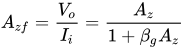
Then the gain of the amplifier with feedback, called the closed-loop gain, AFB is given by
If AOL ≫ 1, then AFB ≈ 1 / β, and the effective amplification (or closed-loop gain) AFB is set by the feedback constant β, and hence set by the feedback network, usually a simple reproducible network, thus making linearizing and stabilizing the amplification characteristics straightforward. If there are conditions where β AOL = −1, the amplifier has infinite amplification – it has become an oscillator, and the system is unstable. The stability characteristics of the gain feedback product β AOL are often displayed and investigated on a Nyquist plot (a polar plot of the gain/phase shift as a parametric function of frequency). A simpler, but less general technique, uses Bode plots.
The combination L = −β AOL appears commonly in feedback analysis and is called the loop gain. The combination (1 + β AOL) also appears commonly and is variously named as the desensitivity factor, return difference, or improvement factor.[10]

Feedback can be used to extend the bandwidth of an amplifier at the cost of lowering the amplifier gain.[15] Figure 2 shows such a comparison. The figure is understood as follows. Without feedback the so-called open-loop gain in this example has a single-time-constant frequency response given by
where fC is the cutoff or corner frequency of the amplifier: in this example fC = 104 Hz, and the gain at zero frequency A0 = 105 V/V. The figure shows that the gain is flat out to the corner frequency and then drops. When feedback is present, the so-called closed-loop gain, as shown in the formula of the previous section, becomes
The last expression shows that the feedback amplifier still has a single-time-constant behavior, but the corner frequency is now increased by the improvement factor (1 + β A0), and the gain at zero frequency has dropped by exactly the same factor. This behavior is called the gain–bandwidth tradeoff. In Figure 2, (1 + β A0) = 103, so AFB(0) = 105 / 103 = 100 V/V, and fC increases to 104 × 103 = 107 Hz.
When the close-loop gain has several poles, rather than the single pole of the above example, feedback can result in complex poles (real and imaginary parts). In a two-pole case, the result is peaking in the frequency response of the feedback amplifier near its corner frequency and ringing and overshoot in its step response. In the case of more than two poles, the feedback amplifier can become unstable and oscillate. See the discussion of gain margin and phase margin. For a complete discussion, see Sansen.[16]
A principal idealization behind the formulation of the Introduction is the network's division into two autonomous blocks (that is, with their own individually determined transfer functions), a simple example of what often is called "circuit partitioning",[17] which refers in this instance to the division into a forward amplification block and a feedback block. In practical amplifiers, the information flow is not unidirectional as shown here.[18] Frequently these blocks are taken to be two-port networks to allow inclusion of bilateral information transfer.[19][20] Casting an amplifier into this form is a non-trivial task, however, especially when the feedback involved is not global (that is directly from the output to the input) but local (that is, feedback within the network, involving nodes that do not coincide with input and/or output terminals).[21][22]

In these more general cases, the amplifier is analyzed more directly without the partitioning into blocks like those in the diagram, using instead some analysis based upon signal-flow analysis, such as the return-ratio method or the asymptotic gain model.[24][25][26] Commenting upon the signal-flow approach, Choma says:[27]
Following up on this suggestion, a signal-flow graph for a negative-feedback amplifier is shown in the figure, which is patterned after one by D'Amico et al..[23] Following these authors, the notation is as follows:
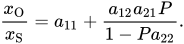
Using this graph, these authors derive the generalized gain expression in terms of the control parameter P that defines the controlled source relationship xj = Pxi:
Combining these results, the gain is given by
To employ this formula, one has to identify a critical controlled source for the particular amplifier circuit in hand. For example, P could be the control parameter of one of the controlled sources in a two-port network, as shown for a particular case in D'Amico et al.[23] As a different example, if we take a12 = a21 = 1, P = A, a22 = –β (negative feedback) and a11 = 0 (no feedforward), we regain the simple result with two unidirectional blocks.

Although, as mentioned in the section Signal-flow analysis, some form of signal-flow analysis is the most general way to treat the negative-feedback amplifier, representation as two two-ports is the approach most often presented in textbooks and is presented here. It retains a two-block circuit partition of the amplifier, but allows the blocks to be bilateral. Some drawbacks of this method are described at the end.
Electronic amplifiers use current or voltage as input and output, so four types of amplifier are possible (any of two possible inputs with any of two possible outputs). See classification of amplifiers. The objective for the feedback amplifier may be any one of the four types of amplifier and is not necessarily the same type as the open-loop amplifier, which itself may be any one of these types. So, for example, an op amp (voltage amplifier) can be arranged to make a current amplifier instead.
Negative-feedback amplifiers of any type can be implemented using combinations of two-port networks. There are four types of two-port network, and the type of amplifier desired dictates the choice of two-ports and the selection of one of the four different connection topologies shown in the diagram. These connections are usually referred to as series or shunt (parallel) connections.[29][30] In the diagram, the left column shows shunt inputs; the right column shows series inputs. The top row shows series outputs; the bottom row shows shunt outputs. The various combinations of connections and two-ports are listed in the table below.
| Feedback amplifier type | Input connection | Output connection | Ideal feedback | Two-port feedback |
|---|---|---|---|---|
| Current | Shunt | Series | CCCS | g-parameter |
| Transresistance | Shunt | Shunt | CCVS | y-parameter |
| Transconductance | Series | Series | VCCS | z-parameter |
| Voltage | Series | Shunt | VCVS | h-parameter |
For example, for a current-feedback amplifier, current from the output is sampled for feedback and combined with current at the input. Therefore, the feedback ideally is performed using an (output) current-controlled current source (CCCS), and its imperfect realization using a two-port network also must incorporate a CCCS, that is, the appropriate choice for feedback network is a g-parameter two-port. Here the two-port method used in most textbooks is presented,[31][32][33][34] using the circuit treated in the article on asymptotic gain model.

Figure 3 shows a two-transistor amplifier with a feedback resistor Rf. The aim is to analyze this circuit to find three items: the gain, the output impedance looking into the amplifier from the load, and the input impedance looking into the amplifier from the source.
The first step is replacement of the feedback network by a two-port. Just what components go into the two-port?
On the input side of the two-port we have Rf. If the voltage at the right side of Rf changes, it changes the current in Rf that is subtracted from the current entering the base of the input transistor. That is, the input side of the two-port is a dependent current source controlled by the voltage at the top of resistor R2.
One might say the second stage of the amplifier is just a voltage follower, transmitting the voltage at the collector of the input transistor to the top of R2. That is, the monitored output signal is really the voltage at the collector of the input transistor. That view is legitimate, but then the voltage follower stage becomes part of the feedback network. That makes analysis of feedback more complicated.

An alternative view is that the voltage at the top of R2 is set by the emitter current of the output transistor. That view leads to an entirely passive feedback network made up of R2 and Rf. The variable controlling the feedback is the emitter current, so the feedback is a current-controlled current source (CCCS). We search through the four available two-port networks and find the only one with a CCCS is the g-parameter two-port, shown in Figure 4. The next task is to select the g-parameters so that the two-port of Figure 4 is electrically equivalent to the L-section made up of R2 and Rf. That selection is an algebraic procedure made most simply by looking at two individual cases: the case with V1 = 0, which makes the VCVS on the right side of the two-port a short-circuit; and the case with I2 = 0. which makes the CCCS on the left side an open circuit. The algebra in these two cases is simple, much easier than solving for all variables at once. The choice of g-parameters that make the two-port and the L-section behave the same way are shown in the table below.
| g11 | g12 | g21 | g22 |
|---|---|---|---|

The next step is to draw the small-signal schematic for the amplifier with the two-port in place using the hybrid-pi model for the transistors. Figure 5 shows the schematic with notation R3 = RC2 || RL and R11 = 1 / g11, R22 = g22.
Figure 3 indicates the output node, but not the choice of output variable. A useful choice is the short-circuit current output of the amplifier (leading to the short-circuit current gain). Because this variable leads simply to any of the other choices (for example, load voltage or load current), the short-circuit current gain is found below.
First the loaded open-loop gain is found. The feedback is turned off by setting g12 = g21 = 0. The idea is to find how much the amplifier gain is changed because of the resistors in the feedback network by themselves, with the feedback turned off. This calculation is pretty easy because R11, RB, and rπ1 all are in parallel and v1 = vπ. Let R1 = R11 || RB || rπ1. In addition, i2 = −(β+1) iB. The result for the open-loop current gain AOL is:
In the classical approach to feedback, the feedforward represented by the VCVS (that is, g21 v1) is neglected.[35] That makes the circuit of Figure 5 resemble the block diagram of Figure 1, and the gain with feedback is then:
where the feedback factor βFB = −g12. Notation βFB is introduced for the feedback factor to distinguish it from the transistor β.

Feedback is used to better match signal sources to their loads. For example, a direct connection of a voltage source to a resistive load may result in signal loss due to voltage division, but interjecting a negative feedback amplifier can increase the apparent load seen by the source, and reduce the apparent driver impedance seen by the load, avoiding signal attenuation by voltage division. This advantage is not restricted to voltage amplifiers, but analogous improvements in matching can be arranged for current amplifiers, transconductance amplifiers and transresistance amplifiers.
To explain these effects of feedback upon impedances, first a digression on how two-port theory approaches resistance determination, and then its application to the amplifier at hand.
Figure 6 shows an equivalent circuit for finding the input resistance of a feedback voltage amplifier (left) and for a feedback current amplifier (right). These arrangements are typical Miller theorem applications.
In the case of the voltage amplifier, the output voltage βVout of the feedback network is applied in series and with an opposite polarity to the input voltage Vx travelling over the loop (but in respect to ground, the polarities are the same). As a result, the effective voltage across and the current through the amplifier input resistance Rin decrease so that the circuit input resistance increases (one might say that Rin apparently increases). Its new value can be calculated by applying Miller theorem (for voltages) or the basic circuit laws. Thus Kirchhoff's voltage law provides:
where vout = Av vin = Av Ix Rin. Substituting this result in the above equation and solving for the input resistance of the feedback amplifier, the result is:
The general conclusion from this example and a similar example for the output resistance case is: A series feedback connection at the input (output) increases the input (output) resistance by a factor ( 1 + β AOL ), where AOL = open loop gain.
On the other hand, for the current amplifier, the output current βIout of the feedback network is applied in parallel and with an opposite direction to the input current Ix. As a result, the total current flowing through the circuit input (not only through the input resistance Rin) increases and the voltage across it decreases so that the circuit input resistance decreases (Rin apparently decreases). Its new value can be calculated by applying the dual Miller theorem (for currents) or the basic Kirchhoff's laws:
where iout = Ai iin = Ai Vx / Rin. Substituting this result in the above equation and solving for the input resistance of the feedback amplifier, the result is:
The general conclusion from this example and a similar example for the output resistance case is: A parallel feedback connection at the input (output) decreases the input (output) resistance by a factor ( 1 + β AOL ), where AOL = open loop gain.
These conclusions can be generalized to treat cases with arbitrary Norton or Thévenin drives, arbitrary loads, and general two-port feedback networks. However, the results do depend upon the main amplifier having a representation as a two-port – that is, the results depend on the same current entering and leaving the input terminals, and likewise, the same current that leaves one output terminal must enter the other output terminal.
A broader conclusion, independent of the quantitative details, is that feedback can be used to increase or to decrease the input and output impedance.
These resistance results now are applied to the amplifier of Figure 3 and Figure 5. The improvement factor that reduces the gain, namely ( 1 + βFB AOL), directly decides the effect of feedback upon the input and output resistances of the amplifier. In the case of a shunt connection, the input impedance is reduced by this factor; and in the case of series connection, the impedance is multiplied by this factor. However, the impedance that is modified by feedback is the impedance of the amplifier in Figure 5 with the feedback turned off, and does include the modifications to impedance caused by the resistors of the feedback network.
Therefore, the input impedance seen by the source with feedback turned off is Rin = R1 = R11 || RB || rπ1, and with the feedback turned on (but no feedforward)
where division is used because the input connection is shunt: the feedback two-port is in parallel with the signal source at the input side of the amplifier. A reminder: AOL is the loaded open loop gain found above, as modified by the resistors of the feedback network.
The impedance seen by the load needs further discussion. The load in Figure 5 is connected to the collector of the output transistor, and therefore is separated from the body of the amplifier by the infinite impedance of the output current source. Therefore, feedback has no effect on the output impedance, which remains simply RC2 as seen by the load resistor RL in Figure 3.[36][37]
If instead we wanted to find the impedance presented at the emitter of the output transistor (instead of its collector), which is series connected to the feedback network, feedback would increase this resistance by the improvement factor ( 1 + βFB AOL).[38]
The gain derived above is the current gain at the collector of the output transistor. To relate this gain to the gain when voltage is the output of the amplifier, notice that the output voltage at the load RL is related to the collector current by Ohm's law as vL = iC (RC2 || RL). Consequently, the transresistance gain vL / iS is found by multiplying the current gain by RC2 || RL:
Similarly, if the output of the amplifier is taken to be the current in the load resistor RL, current division determines the load current, and the gain is then:

Some drawbacks of the two two-port approach follow, intended for the attentive reader.
Figure 7 shows the small-signal schematic with the main amplifier and the feedback two-port in shaded boxes. The feedback two-port satisfies the port conditions: at the input port, Iin enters and leaves the port, and likewise at the output, Iout enters and leaves.
Is the main amplifier block also a two-port? The main amplifier is shown in the upper shaded box. The ground connections are labeled. Figure 7 shows the interesting fact that the main amplifier does not satisfy the port conditions at its input and output unless the ground connections are chosen to make that happen. For example, on the input side, the current entering the main amplifier is IS. This current is divided three ways: to the feedback network, to the bias resistor RB and to the base resistance of the input transistor rπ. To satisfy the port condition for the main amplifier, all three components must be returned to the input side of the main amplifier, which means all the ground leads labeled G1 must be connected, as well as emitter lead GE1. Likewise, on the output side, all ground connections G2 must be connected and also ground connection GE2. Then, at the bottom of the schematic, underneath the feedback two-port and outside the amplifier blocks, G1 is connected to G2. That forces the ground currents to divide between the input and output sides as planned. Notice that this connection arrangement splits the emitter of the input transistor into a base-side and a collector-side – a physically impossible thing to do, but electrically the circuit sees all the ground connections as one node, so this fiction is permitted.
Of course, the way the ground leads are connected makes no difference to the amplifier (they are all one node), but it makes a difference to the port conditions. This artificiality is a weakness of this approach: the port conditions are needed to justify the method, but the circuit really is unaffected by how currents are traded among ground connections.
However, if no possible arrangement of ground conditions leads to the port conditions, the circuit might not behave the same way.[39] The improvement factors (1 + βFB AOL) for determining input and output impedance might not work.[40] This situation is awkward, because a failure to make a two-port may reflect a real problem (it just is not possible), or reflect a lack of imagination (for example, just did not think of splitting the emitter node in two). As a consequence, when the port conditions are in doubt, at least two approaches are possible to establish whether improvement factors are accurate: either simulate an example using Spice and compare results with use of an improvement factor, or calculate the impedance using a test source and compare results.
A more practical choice is to drop the two-port approach altogether, and use various alternatives based on signal flow graph theory, including the Rosenstark method, the Choma method, and use of Blackman's theorem.[41] That choice may be advisable if small-signal device models are complex, or are not available (for example, the devices are known only numerically, perhaps from measurement or from SPICE simulations).
Summarizing the two-port analysis of feedback, one can get this table of formulas.[34]
| Feedback Amplifier | Source Signal | Output Signal | Transfer Function | Input Resistance | Output Resistance |
|---|---|---|---|---|---|
| Series-Shunt (voltage amplifier) | Voltage | Voltage | |||
| Shunt-Series (current amplifier) | Current | Current | |||
| Series-Series(transconductance amplifier) | Voltage | Current | |||
| Shunt-Shunt (transresistance amplifier) | Current | Voltage |
The variables and their meanings are
- gain, - current, - voltage,- feedback gain and - resistance.
The subscripts and their meanings are
- feedback amplifier, - voltage,- transconductance, - transresistance, - output and - current for gains and feedback and - input for resistances.
For example means voltage feedback amplifier gain.[34]
Simple amplifiers like the common emitter configuration have primarily low-order distortion, such as the 2nd and 3rd harmonics. In audio systems, these can be minimally audible because musical signals are typically already a harmonic series, and the low-order distortion products are hidden by the masking effect of the human hearing system.[42][43]
After applying moderate amounts of negative feedback (10–15 dB), the low-order harmonics are reduced, but higher-order harmonics are introduced.[44] Since these are not masked as well, the distortion becomes audibly worse, even though the overall THD may go down.[44] This has led to a persistent myth that negative feedback is detrimental in audio amplifiers,[45] leading audiophile manufacturers to market their amplifiers as "zero feedback" (even when they use local feedback to linearize each stage).[46][47]
However, as the amount of negative feedback is increased further, all harmonics are reduced, returning the distortion to inaudibility, and then improving it beyond the original zero-feedback stage (provided the system is strictly stable).[48][45][49] So the problem is not negative feedback, but insufficient amounts of it.
β is the feedback loop attenuation, or feedback factor ... noise gain is equal to 1/β
dividing a circuit into smaller parts ...[so]...the number of connections between parts is minimized
In real cases, unfortunately, blocks...cannot be assumed to be unidirectional.
{{cite journal}}: CS1 maint: multiple names: authors list (link)
editions:BZ69IvJlfW8C.
Great care must be exercised in applying two-port theory to ensure that the amplifier feedback networks can actually be represented as two-ports
most of the harmonic distortion has been masked, however, a couple of the high order harmonics were far enough away in frequency and loud enough to be heard. So in order to determine the audibility of harmonic distortion, we have to know how much masking is done by different tones at different loudness levels.
Masking is a principle concept in the perception of distortion, as distortion products will only contribute to the percept of distortion if they are not masked by the primary stimulus or other distortion products.
Here we see that as low feedback figures are applied to a single gain stage the 2nd harmonic declines linearly with feedback, but increased amounts of higher order harmonics are created. As feedback increases above about 15 dB or so, all these forms of distortion [decline] in proportion to increased feedback.
Of course this experiment gives the impression that more feedback is worse. You have to get past that bump. Hardly anybody who has ever tried it like this has actually heard the inevitable (and frankly magical) improvement that happens once you do get beyond, say 20 or 30dB. From there on you get an unambiguous net improvement that goes on forever.
Dreadnaught III uses no global negative feedback.
Source: Wikipedia. Article content is retrieved live through the MediaWiki API.

A negative-feedback amplifier (or feedback amplifier) is an electronic amplifier that subtracts a fraction of its output from its input, so that negative feedback opposes the original signal. The applied negative feedback can improve its performance (gain stability, linearity, frequency response, step response) and reduces sensitivity to parameter variations due to manufacturing or environment. Because of these advantages, many amplifiers and control systems use negative feedback. An idealized negative-feedback amplifier as shown in the diagram is a system of three elements (see Figure 1): an amplifier with gain AOL, a feedback network β, which senses the output signal and possibly transforms it in some way (for example by attenuating or filtering it), a summing circuit that acts as a subtractor (the circle in the figure), which combines the input and the transformed output.

An operational amplifier (often op amp, op-amp, or opamp) is a DC-coupled electronic amplifier with a differential input, a (usually) single-ended output voltage, and an extremely high gain. Its name comes from its original use of performing mathematical operations in analog computers. The voltage-feedback opamp (VFOA or VFA, the focus of this article) amplifies the voltage difference between its two inputs, while the less common current-feedback op amp (CFOA) amplifies the current between its two inputs. By using negative feedback, the characteristics of an op amp application circuit (e.g., its gain, input and output impedance, bandwidth, and functionality) can be determined by external components and have little dependence on temperature coefficients or engineering tolerance in the op amp itself. This flexibility has made the op amp a popular building block in analog circuits. Today, op amps are used widely in consumer, industrial, and scientific electronics. Many standard integrated circuit op amps cost only a few cents; however, some integrated or hybrid operational amplifiers with special performance specifications may cost over US$100. Op amps may be packaged as components or used as elements of more complex integrated circuits. The op amp is one type of differential amplifier. Other differential amplifier types include the fully differential amplifier (an op amp with a differential rather than single-ended output), the instrumentation amplifier (usually built from three op amps), the isolation amplifier (with galvanic isolation between input and output), and negative-feedback amplifier (usually built from one or more op amps and a resistive feedback network).
Harold Stephen Black (April 14, 1898 – December 11, 1983) was an American electrical engineer, who revolutionized the field of applied electronics by inventing the negative feedback amplifier in 1927. To some, his invention is considered the most important breakthrough of the twentieth century in the field of electronics, since it has a wide area of application. This is because all electronic devices (vacuum tubes, bipolar transistors and MOS transistors) are inherently nonlinear, but they can be made substantially linear with the application of negative feedback. Negative feedback works by sacrificing gain for higher linearity (or in other words, smaller distortion/intermodulation). By sacrificing gain, it also has an additional effect of increasing the bandwidth of the amplifier. However, a negative feedback amplifier can be unstable such that it may oscillate. Once the stability problem is solved, the negative feedback amplifier is extremely useful in the field of electronics. Black published a famous paper, Stabilized feedback amplifiers, in 1934.

An instrumentation amplifier (sometimes shorthanded as in-amp or InAmp) is a precision differential amplifier that has been outfitted with input buffer amplifiers, which eliminate the need for input impedance matching and thus make the amplifier particularly suitable for use in measurement and test equipment. Additional characteristics include very low DC offset, low drift, low noise, very high open-loop gain, very high common-mode rejection ratio, and very high input impedances. Instrumentation amplifiers are used where great accuracy and stability of the circuit both short- and long-term are required. Although the instrumentation amplifier is usually shown schematically identical to a standard operational amplifier (op-amp), the electronic instrumentation amplifier is almost always internally composed of 3 op-amps. These are arranged so that there is one op-amp to buffer each input (+, −), and one to produce the desired output with adequate impedance matching for the function. While the instrumentation amplifier is optimized for the task of precise amplification of high-impedance voltage signals, this design choice comes at the cost of flexibility: the instrumentation amplifier is thus not intended to perform integration, differentiation, rectification, or any other non-voltage-gain function, which are best left to op-amps. The most commonly used instrumentation amplifier circuit is shown in the figure. The gain of the circuit is A v = V out V 2 − V 1 = ( 1 + 2 R 1 R gain ) R 3 R 2 . {\displaystyle A_{v}={\frac {V_{\text{out}}}{V_{2}-V_{1}}}=\left(1+{\frac {2R_{1}}{R_{\text{gain}}}}\right){\frac {R_{3}}{R_{2}}}.} The rightmost amplifier, along with the resistors labelled R 2 {\displaystyle R_{2}} and R 3 {\displaystyle R_{3}} is just the standard differential-amplifier circuit, with gain R 3 / R 2 {\displaystyle R_{3}/R_{2}} and differential input resistance 2 ⋅ R 2 {\displaystyle 2\cdot R_{2}} . The two amplifiers on the left are the buffers. With R gain {\displaystyle R_{\text{gain}}} removed (open-circuited), they are simple unity-gain buffers; the circuit will work in that state, with gain simply equal to R 3 / R 2 {\displaystyle R_{3}/R_{2}} and high input impedance because of the buffers. The buffer gain could be increased by putting resistors between the buffer inverting inputs and ground to shunt away some of the negative feedback; however, the single resistor R gain {\displaystyle R_{\text{gain}}} between the two inverting inputs is a much more elegant method: it increases the differential-mode gain of the buffer pair while leaving the common-mode gain equal to 1. This increases the common-mode rejection ratio (CMRR) of the circuit and also enables the buffers to handle much larger common-mode signals without clipping than would be the case if they were separate and had the same gain. Another benefit of the method is that it boosts the gain using a single resistor rather than a pair, thus avoiding a resistor-matching problem and very conveniently allowing the gain of the circuit to be changed by changing the value of a single resistor. A set of switch-selectable resistors or even a potentiometer can be used for R gain {\displaystyle R_{\text{gain}}} , providing easy changes to the gain of the circuit, without the complexity of having to switch matched pairs of resistors. The ideal common-mode gain of an instrumentation amplifier is zero. In the circuit shown, common-mode gain is caused by mismatch in the resistor ratios R 2 / R 3 {\displaystyle R_{2}/R_{3}} and by the mismatch in common-mode gains of the two input op-amps. Obtaining very closely matched resistors is a significant difficulty in fabricating these circuits, as is optimizing the common-mode performance. An instrumentation amplifier can also be built with two op-amps to save on cost, but the gain must be higher than two (+6 dB). Instrumentation amplifiers can be built with individual op-amps and precision resistors, but are also available in integrated circuit form from several manufacturers (including Texas Instruments, Analog Devices, and Renesas Electronics). An IC instrumentation amplifier typically contains closely matched laser-trimmed resistors, and therefore offers excellent common-mode rejection. Examples include INA128, AD8221, LT1167 and MAX4194. Instrumentation amplifiers can also be designed using "indirect current-feedback architecture", which extend the operating range of these amplifiers to the negative power supply rail, and in some cases the positive power supply rail. This can be particularly useful in single-supply systems, where the negative power rail is simply the circuit ground (GND). Examples of parts utilizing this architecture are MAX4208/MAX4209 and AD8129/AD8130 Archived 11 November 2014 at the Wayback Machine.
Before the 1921 destruction of Tulsa’s Greenwood District, Black residents had created a remarkable center of business and community life. The district included stores, professional offices, entertainment venues and homes owned by Black citizens. Understanding Greenwood means learning what was built—not only what was burned.
MORE →Brown v. Board of Education in 1954.